Entertainment
Understanding Chip Lithography: The Process Behind Microelectronics
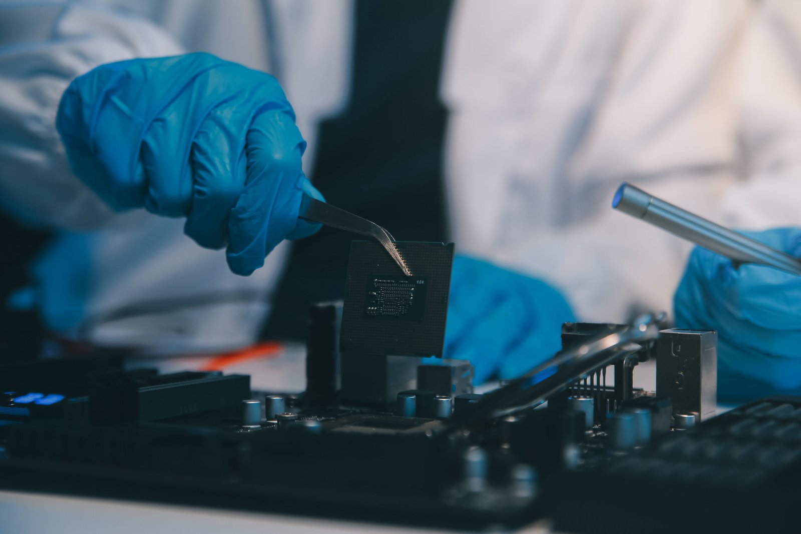
The marvels of present day technology, from powerful computers to smooth smartphones, owe tons in their life to advancements in chip lithography. This foundational procedure in semiconductor manufacturing is what permits the introduction of included circuits, the tiny brains in the back of our favourite devices.
What is Chip Lithography?
Chip lithography, often referred to as photolithography, is a process used in semiconductor manufacturing to sample circuits onto a silicon wafer. Think of it as a high-tech model of stenciling. Using light, specialised device, and chemicals, manufacturers can create the microscopic structures that shape the transistors, resistors, and different additives of a chip.
These systems are measured in nanometers (nm), with today’s contemporary chips proposing functions as small as 3nm. To placed that into perspective, a single nanometer is one-billionth of a meter—thousands of times smaller than the width of a human hair!
The Importance of Chip Lithography
Chip lithography isn’t only a manufacturing step—it’s a riding pressure in the back of technological innovation. Here are some motives why it’s essential:
- Miniaturization of Technology
The ability to produce smaller and more green chips has revolutionized electronics. Devices today are faster, lighter, and greater compact way to advancements in lithography. - Moore’s Law and Progress
- Lithography has played a applicable feature in keeping Moore’s Law alive. This principle, which predicts the doubling of transistors on a chip approximately each years, is predicated on ever-smaller lithography techniques.
- Three. Cost Efficiency
- While lithography gadget is high-priced, the method itself allows the manufacturing of lots and lots of chips from a unmarried wafer, using down the rate consistent with unit and making era accessible to the loads.
- Four. Enabling AI and Advanced Computing
- High-typical overall performance computing, artificial intelligence, and cloud offerings all depend on superior chips made possible thru contemporary lithography.
- The Lithography Process: Step-via-Step
- To understand chip lithography better, allow’s stroll through its key steps:
- Wafer Preparation
The approach starts with a wafer, generally manufactured from silicon, which serves as the substrate for the chip. The wafer is wiped easy and polished to create a easy floor, making sure maximum excellent precision throughout lithography. - Coating with Photoresist
A slight-touchy material known as photoresist is carried out to the wafer. This skinny film reacts to ultraviolet (UV) mild, permitting selective areas to be hardened or dissolved primarily based at the publicity sample. - Three. Mask Alignment
- A photomask or reticle is placed over the wafer. This masks consists of the problematic pattern of the circuit format, with a view to be transferred to the wafer.
- Exposure to UV Light
The wafer is uncovered to UV slight, which shines via the masks. The mild alters the homes of the photoresist, correctly “printing” the circuit sample onto the wafer. - Development of the Pattern
After exposure, the wafer undergoes a development technique to dispose of both the exposed or unexposed photoresist (depending on whether or not a great or terrible withstand is used). This step well-knownshows the pattern etched into the photoresist layer. - Etching and Deposition
Using the patterned photoresist as a manual, layers of the wafer are etched away or materials are deposited to build the real circuit. Etching can be achieved chemically or with plasma. - Photoresist Removal
The final photoresist is stripped away, leaving the finished sample. The wafer is now ready for in addition processing, together with layering and repeating the lithography way for introduced circuit abilties. - Technological Advancements in Lithography
- The lithography subject is constantly evolving, with new technologies growing to address its challenges. Some excellent advancements encompass:
- Extreme Ultraviolet (EUV) Lithography
EUV lithography makes use of shorter wavelengths of mild (13.5nm) to achieve finer patterns. This modern generation is critical for generating chips with features smaller than 7nm. - Directed Self-Assembly (DSA)
DSA leverages the natural houses of substances to shape patterns on the nanoscale, imparting a functionality possibility to standard photolithography. - Three. Multi-Patterning Techniques
- To triumph over limitations in choice, manufacturers often use more than one patterning steps, together with double or quadruple patterning, to attain the preferred element.
- Four. AI in Process Optimization
- Artificial intelligence is more and more getting used to optimize lithography strategies, decreasing mistakes and improving efficiency.
- Challenges in Lithography
- As with any advanced technology, lithography comes with its demanding situations:
- Precision and Complexity
Creating skills at the nanometer scale calls for excessive precision. Any errors throughout lithography can result in faulty chips, making notable control crucial. - Cost of Equipment
State-of-the-art lithography machines, consisting of those using excessive ultraviolet (EUV) generation, can cost masses of hundreds of heaps of dollars. This cost poses a barrier for smaller producers. - Three. Material Limitations
- As functions get smaller, new substances and strategies are desired to conquer physical obstacles. For example, conventional photomasks won’t suffice for next-era chips.
- Four. Heat and Power Challenges
- Smaller chips frequently generate greater warmness, requiring progressive cooling and power control solutions to keep general performance and reliability.
- Applications of Lithography
- Semiconductor ICs: Lithography is essential for the production of semiconductor integrated circuits, enabling the creation of processors, memory chips, and other vital components that form the backbone of modern electronics.
- Microelectromechanical Systems (MEMS): Lithography plays a crucial role in manufacturing MEMS devices, which are used in sensors and actuators for industries such as automotive and healthcare.
- Emerging Technologies: Lithography is also driving progress in emerging fields like quantum computing, photonics, and nanotechnology, playing a key role in their development.
- The Future of Lithography
- The semiconductor industry is at the cutting edge of innovation, with ongoing research dedicated to next-generation lithographic techniques. Potential advancements include:
- Directed Self-Assembly (DSA): Harnessing molecular self-agency for pattern formation.
- X-ray Lithography: Promises even shorter wavelengths than EUV for extremely-best resolutions.
- Free Electron Lasers (FEL): Exploring coherent light sources for high precision.
- As the call for for effective, strength-efficient devices grows, chip lithography will remain a cornerstone of technological development. Researchers are already exploring the capacity of sub-nanometer capabilities, quantum computing-well suited lithography, or even 3-d lithographic techniques.
- These improvements could redefine what’s feasible in electronics, beginning the door to innovations we are able to most effective imagine nowadays.
- Conclusion
- Chip lithography is greater than just a production procedure—it’s a testament to human ingenuity and precision engineering. From its foundational steps to its function in driving technological innovation, lithography stands on the heart of modern electronics.
- Whether you’re an aspiring tech fanatic or someone eager on know-how the nuts and bolts of the gadgets we use each day, delving into chip lithography offers a charming glimpse into the world of semiconductors and the destiny of era.


